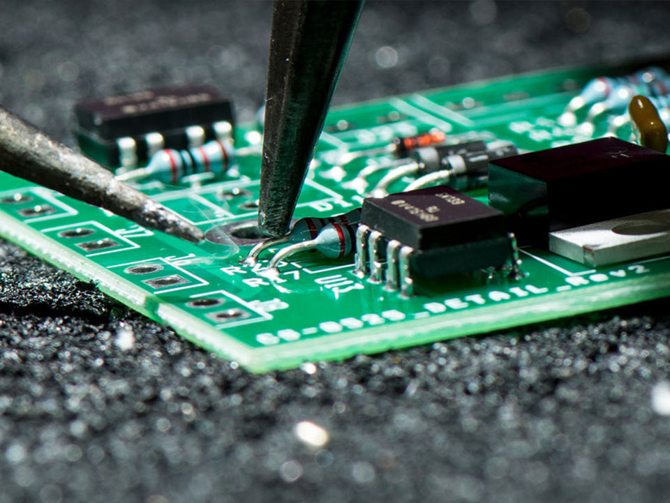
柔性 PCB 最简单的
成本降低是什么?
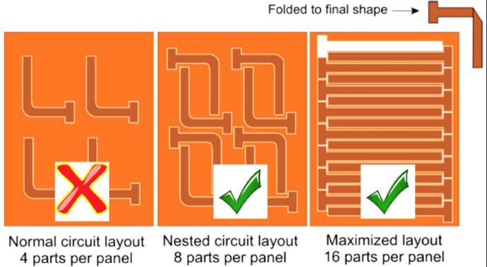
Did you know that material utilization is one of the biggest cost drivers on flex PCB?
Nesting circuits and maximising
the panelization will result in huge cost savings.
See the example below. A panel with a normal circuit layout with 4 parts, can with nested circuit layout give a 50% increase of parts per panel, and by maximizing the circuit layout improve even more, thus result in huge cost savings.
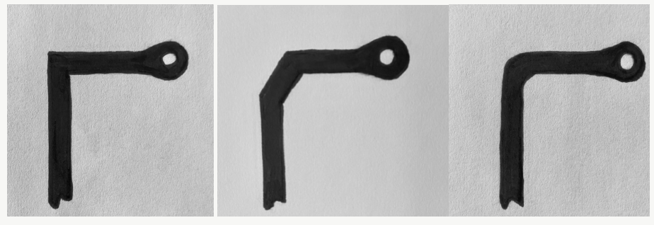
So, how should the conductor routing be?
- Conductors should not be placed directly over each other. ( z-axis )
- The number of layers in the bend area should be kept to a minimum.
- Vias & PTHs in bend areas should be avoided.
- Curved tracks are preferable.
- Tracks/Gaps should be uniform.
Something to remember when you look into cost savings on your flex PCB design. We have been involved in thousands of Flex and Flex-Rigid designs over the year.
Feel free to reach out to us when you are designing a product in need of any of these. On of our Technical Advisors might be able to assist, and see solutions not considered before.
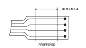
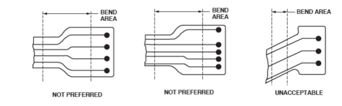
They have sketched up the best, better and the one conductor routing to avoid, below.
AVOID BETTER BEST
成本降低是什么?


Leave a Reply
Want to join the discussion?Feel free to contribute!