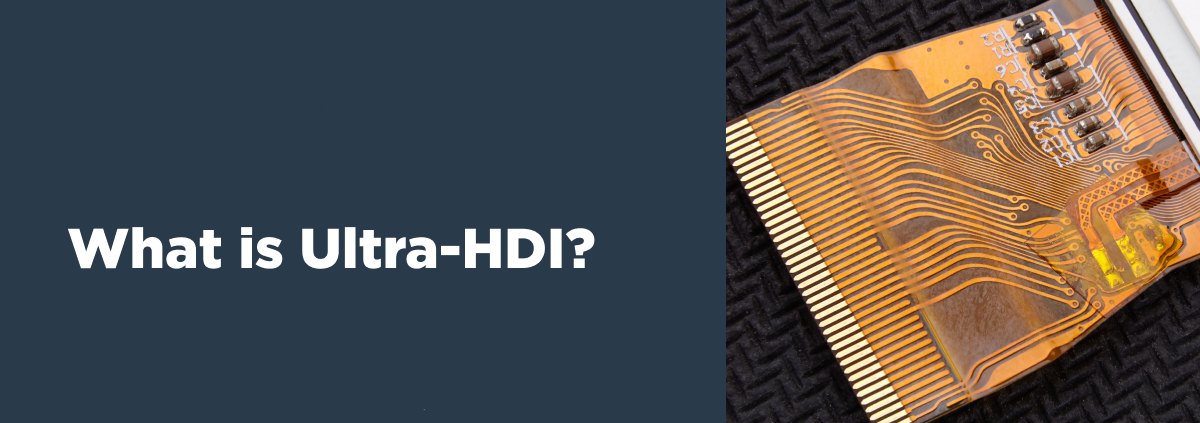
What is Ultra-HDI?

There is a lot of conversation about “Ultra-HDI” especially with all of the anticipated work being done as part of the CHIPS Act.  In my experience, Ultra-HDI means different things to different people depending on where their capabilities and expertise are.  IPC has created a working group to address ultra-HDI and their position is that to be considered ultra-HDI, a design needs to include one or more of the following parameters:
Line width below 50 microns

  • Spacing below 50 microns
  • Dielectric thickness below 50 microns
  • Micro via diameter below 75 microns

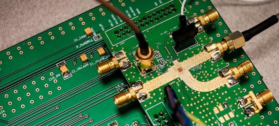
That is a pretty generous definition and there are a few specialized fabricators today that can produce printed circuit boards that meet this criteria using the traditional subtractive etch processes. While using a 50 micron trace and space is an improvement over the traditional 75 micron minimums that we have historically been limited to, I think where it becomes much more interesting is when we are now seeing fabricators that have the capability to create layers with 15 micron line and space. Several fabricators are now building with semi-additive PCB fabrication techniques (SAP) including fabricators that specialize in high-mix low volume work.  We have traditionally seen SAP processes run in primarily high-volume facilities.

Even if we don’t push the boundary all the way to 15 micron, using a 25 micron trace and space to break out of tight BGA areas has so many benefits:

  • Dramatic size and weight reduction over current state-of-the-art
  • Tight spacing and impedance control (< 5%) for all line widths, from 15 microns and above
  • Reduced layer count, micro vias and lamination cycles – for greater reliability
  • Aspect ratios greater than 1:1 for metal traces – for improved signal integrity
  • RF performance better than traditional subtractive-etch processes
  • Reduced costs – especially for complex, high-performance boards

In a previous blog post, we discussed a few of the frequently asked questions as printed circuit board designers navigate the learning curve when doing their first designs utilizing these new capabilities.  There is a link included below if you want to check those out.

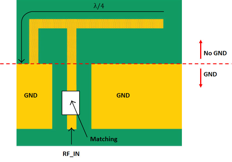
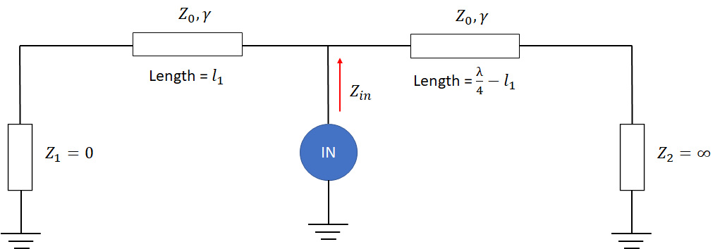
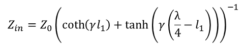
In this blog, we will continue with a few more frequently asked questions with a design for manufacturability focus.  For this discussion, let’s look at applications where printed circuit board designers are using a hybrid-approach to their designing.  Certain layers are routed with a 25 micron trace and space to reduce the number of layers needed to route out of tight BGA areas and power and ground layers have much larger features.  These power and ground layers are typically produced with subtractive-etch processes.  When this approach is used, a common question being asked is:

Can I design Via-In-Pad-Plated-Over (VIPPO) technology with these ultra-fine lines and spaces?

The short answer is yes, with the following guidelines:  Via in pad/ plated over structures should be run on non-ultra-high-density layers.  Preferably these structures, if needed, should be used in an external power/ground structure with line width of 75 micron (3 mils) and spacing of 125 micron (5 mils).  This is due to the multiple plating processes required to produce VIPPO technology.

If via-in-pad is necessary along with the ultra-fine lines externally, then a copper filled micro via should be used to route to the next layer down.  This via diameter should be 3 to 4 mils diameter and the dielectric spacing should be no greater than the via diameter, preferably less.

A buried structure may be used if the top and bottom layers of the subassembly do not use ultra-fine line width technology.  This via may be filled and plated over.

What is the minimum spacing from trace to pad?

While the copper to copper spacing can add costs in subtractive etch processing, in the semi-additive environment this is not the case.

With inner layers, spacing could be 25 microns or below depending on the technology being used by the PCB fabricator.

With outer layers, there must be enough space to allow the solder mask to fully cover the trace and not expose any copper.  “Mask defined” pads are recommended over “metal defined” pads.  This will prevent solder mask registration issues exposing the adjacent metal when the external spacing is less than 75 microns between the pad and adjacent metal.

In comparison to the build-up of a PCB, the stackup is more concerned with the electrical type of each layer. Material thicknesses or what dielectrics are used is of less importance than which layers are dedicated to what, such as signal (SIG) layers, ground (GND) layers, or power (PWR) layers.

Table

Description automatically generated

Signal layers contain predominantly signal-carrying traces (sometimes with routed power or copper pours), whereas power and ground layers are typically completely solid copper pours over the entire layer. Ground layers are used for reference of the signal layers and their return paths, and a power layer is either a solid, continuous power plane of a certain voltage or several islands or copper pours of various different voltage levels.

Before routing a PCB, we want to determine our stackup, which depends on the number of layers we have available. Then, we want to go through the layers one-by-one, assigning ground, power, or signals to individual layers.

Combinations are of course also possible—we can mix power and ground, signal and ground or signal and power.

Ground Layer

One of the most important layer types is the ground layer. This layer type is used predominantly as a reference plane or layer for signal (and power) trace return paths. For every forward path, we need a return path to complete the loop.

Power Layer

A power layer is used for power distribution. Keep in mind that for low-speed and low-bandwidth systems it isn’t entirely critical, and you can route your power with traces on signal layers. However, power planes and layers become increasingly important in terms of power delivery for high-speed circuits. Additionally, if coupled with a ground layer on a closely spaced, adjacent plane, these form a type of parallel plate capacitor.

Signal Layer

Lastly, we have our signal layer where we will route our traces, effectively forming our signal forward path. As seen before, we can use a ground layer or in certain cases even a power layer as a reference for our return path.

Return Paths and References

Now the question is, how do we assign layer types in a PCB in a sensible way? We have certain goals for EMI performance, signal and power integrity, and we want a systematic approach to deciding the stackup. We don’t want to just arbitrarily assign different layer types.

There are a couple golden rules. Firstly, for AC signals in the region of a couple of kHz, the return path is not the shortest path but rather the path directly underneath the trace (forward path). This is the part with the least impedance. For example, for a trace on a top signal layer and a ground plane directly below on layer two, the forward path is on the signal layer, and the return path is directly below that trace in the ground plane beneath.

Another thing to consider is that the signal energy flows in the dielectric space between the copper (trace and plane). The copper therefore is simply a waveguide. For good signal integrity and EMI performance, we need to take into account both the forward and the return path, where the signal energy is flowing, and how it is bound between the forward and return paths.

In essence, close couplings between signal and ground planes and power and ground planes is desired in order to prevent fields from spreading. Our main goal is to avoid fields from spreading, as spreading fields lead coupling from signals to signal, which leads to crosstalk. Spreading fields also mean some form of radiation, which leads to EMI issues.

Assigning Layers and Layer Pairs

How do we avoid fields from spreading, and how do we contain these fields?

The main thing we as PCB design engineers need to keep in mind, is that every forward signal or power path needs a closely coupled reference. In addition, for high-speed or higher-energy signals, it makes sense to also use stripline instead of microstrip traces. Stripline means that we have a signal trace sandwiched between two ground planes, providing good field coupling from the signal to both of the ground planes on either side.

As stated previously, another point to consider is adjacent power and ground planes. This is to improve power delivery at high frequencies where SMD capacitors (even ones in small packages) start to look inductive.

In essence, when designing a stackup, follow the simple rule of having a minimum of one ground reference layer closely adjacent to any signal or power layer, and you should be pretty safe to start.

Recommended Multilayer Stackups

Finally, here are some of my favourite multilayer stackups that follow the guidelines we previously outlined.

Four-layer (routed power): SIG – GND – GND – SIG

Six-layer: SIG – GND – SIG – PWR – GND – SIG

Eight-layer: SIG – GND – SIG – PWR – GND – SIG – GND – SIG

A picture containing table

Description automatically generated

Printed antennas are a very popular option for RF PCBs as they maintain the low profile of a planar device. If you look at some Bluetooth/WiFi capable MCUs, you will likely see an inverted-F antenna along the board edge to provide Rx and Tx in a compact form factor. In this article, I’ll show how to design one of these antennas, including some design equations, and where to place these antennas for maximum radiation efficiency without interference into other circuits.

Inverted-F Antenna Overview

The typical implementation of an inverted-F antenna is shown in the image below. This type of antenna is a quarter-wavelength antenna where the operational parameters (bandwidth, impedance, etc.) are set by adjusting the geometry along the quarter-wavelength leg of the antenna. An overview of a typical inverted-F antenna is shown below.

inverted F antenna
The GND plane on L2 should run right to the edge of the GND on L1, and no copper pour should be below the antenna. This allows the antenna to radiate nearly omnidirectionally around the longer leg of the antenna where the current is non-zero. Although the radiation is omnidirectional and provided by fringing fields, this reduces the gain one would expect from this type of antenna. Thanks to their near omnidirectionality, these antennas were formerly the most popular for use as single-band or dual-band antennas in older mobile handsets.

A variation on this is the meandered inverted-F antenna or MIFA. This antenna is most commonly seen in the ESP8266 module, which uses the well-known ESP32 MCU. The meandered antenna is on the top layer and it includes a long zig-zagging segment making up the quarter-wave section of the antenna.

Both of these antennas can be compared to patch antennas, and the inverted-F antenna (or its variants) offers several advantages over a basic patch antenna:

  • Inverted-F antennas are smaller than patch antennas operating at the same wavelength
  • Inverted-F antennas can be probe-fed or direct-fed as long as a matching network is present
  • Inverted-F antennas can be made multiband by applying more branches
  • Inverted-F antenna bandwidths are comparable, but bandwidths can be more easily tuned with passives

The main disadvantage is the lower gain compared to a patch antenna because patch antennas emit into the half-plane above the ground region. The other disadvantage is that you cannot form inverted-F antennas into groups as you would with a patch antenna array. Therefore, for more advanced antenna systems, patch antennas have dominated.

Inverted-F Antenna Design Equations

Unfortunately, there are no design equations for an inverted-F antenna due to its typically complex structure. However, because it is constructed from transmission lines, we can take a circuit-based approach to calculate the input impedance for a given microstrip width.

First, the designer has the freedom to select the microstrip impedance to be used in the inverted-F antenna design. There is no strict requirement for a particular width of microstrip, but it should be noted that the impedance could be very large, even surpassing propagating wave impedance values in vacuum or dielectrics.

Although the characteristic impedance of the trace sections is difficult to determine, the propagation constant and total antenna length are easy to determine based on the quarter wavelength target and the target frequency:

inverted F antenna

Once the propagation constant is known, the input impedance into the antenna can be calculated with a circuit model as long as the trace impedance is known. The circuit model below shows the two branches in the standard inverted-F antenna arrangement, where one leg is shorted (Z1 = 0 Ohms) and the other leg is open (Z2 = infinity).

inverted F antenna circuit model

If you set these two legs in parallel and use the standard input impedance equation for each leg, you will find the following result for the antenna’s input impedance:

inverted-F input impedance

Once the input impedance is known, it can then be matched to the antenna feedline with an LC impedance matching network.

Component or Copper Fill?

When working in your PCB layout software, should you create your inverted-F antenna as a component or as copper fill regions? There are good reasons to do both, and you will get the same result in either case. Personally, I prefer to use a component to create an inverted-F antenna, but this has to be done to match a specific outer layer thickness and Dk value.

To create an inverted-F antenna as a component, place each of the copper elements in the antenna and poured into the component footprint. Once the antenna is placed into the PCB layout, it will be easier to move and rotate the antenna. Make sure to define the component as a Net Tie to prevent any short circuit errors and to avoid questions from your fabricator. The downside of this is that, if there are any updates needed to the antenna, these need to be made to the footprint, and then the footprint needs to be updated in the PCB layout.

inverted F antenna Altium
Inverted-F antenna as a component footprint created with copper fills. Pads are assigned at the two legs of the antenna.

To complete this component, place a single pad as input at the feedline entry on the antenna that matches the pin on the schematic symbol. Then wire the component up in a schematic just like you would other components. Once the components are updated into the PCB, the inverted-F antenna footprint will appear, and it can be placed and routed just like other components.

Did you know that material utilization is one of the biggest cost drivers on flex PCB?

Nesting circuits and maximising
the panelization will result in huge cost savings.

See the example below. A panel with a normal circuit layout with 4 parts, can with nested circuit layout give a 50% increase of parts per panel, and by maximizing the circuit layout improve even more, thus result in huge cost savings.

So, how should the conductor routing be?

  • Conductors should not be placed directly over each other. ( z-axis )
  • The number of layers in the bend area should be kept to a minimum.

  • Vias & PTHs in bend areas should be avoided.
  • Curved tracks are preferable.
  • Tracks/Gaps should be uniform.

Something to remember when you look into cost savings on your flex PCB design. We have been involved in thousands of Flex and Flex-Rigid designs over the year.
Feel free to reach out to us when you are designing a product in need of any of these. On of our Technical Advisors might be able to assist, and see solutions not considered before.

They have sketched up the best, better and the one conductor routing to avoid, below.

AVOID                                                                                BETTER                                                                      BEST

  1. PCB material types

FR-4

HDI board

Metal core

High tg material

  1. Your electronic project with various PCB material

With the development of electronic technology, the circuit board plays such an important role in electronic products, medical devices, industrial equipment, safety and security equipment and so on. So what kinds of PCB materials you choose will make a great effect on the functionality, manufacturability and life cycle of your board.

FR-4

In fact, FR-4 refers to a grade of material rather than a material, which is a composite material for glass-reinforced epoxy laminate material. FR-4 is made up of woven fiberglass cloth with an epoxy resin binder that is flame resistant. And FR stands for flame retardant, it denotes that the material complies with the standard UL94V-0.

Note: FR-4 material provides the fundamental standard for PCB substrates, keeping a widely effective balance between cost, durability, performance, manufacturability, as well as electrical properties.

Standard FR-4: save product costs and is affordable and effective for many applications.

Metal core: if you are making a electronic project of LED based products, choose the metal core in your boards. What’s more, metal core PCB is more and more common in a variety of lighting applications-for home, workplace, and vehicle.

HDI material: HDI technology is a good solution for smaller and lighter products, high-tech applications, denser BGA and QFP packages, as well as lowered heat transfer included stress.

High TG: If there is a higher power density in electronic products and heat generation will tend to disturbing heat sink or other parts of the products, so high Tg PCB is the best solution. What is more, you can find that high Tg PCBs are applied in electronic industries which can operate in relatively high temperatures as high Tg PCB are more and more popular in recent years.