Inverted-F Antenna Design For a PCB

Inverted-F Antenna Overview
The typical implementation of an inverted-F antenna is shown in the image below. This type of antenna is a quarter-wavelength antenna where the operational parameters (bandwidth, impedance, etc.) are set by adjusting the geometry along the quarter-wavelength leg of the antenna. An overview of a typical inverted-F antenna is shown below.
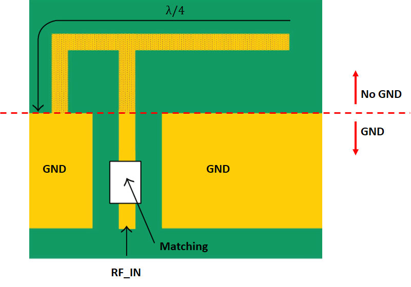
The GND plane on L2 should run right to the edge of the GND on L1, and no copper pour should be below the antenna. This allows the antenna to radiate nearly omnidirectionally around the longer leg of the antenna where the current is non-zero. Although the radiation is omnidirectional and provided by fringing fields, this reduces the gain one would expect from this type of antenna. Thanks to their near omnidirectionality, these antennas were formerly the most popular for use as single-band or dual-band antennas in older mobile handsets.
A variation on this is the meandered inverted-F antenna or MIFA. This antenna is most commonly seen in the ESP8266 module, which uses the well-known ESP32 MCU. The meandered antenna is on the top layer and it includes a long zig-zagging segment making up the quarter-wave section of the antenna.
Both of these antennas can be compared to patch antennas, and the inverted-F antenna (or its variants) offers several advantages over a basic patch antenna:
- Inverted-F antennas are smaller than patch antennas operating at the same wavelength
- Inverted-F antennas can be probe-fed or direct-fed as long as a matching network is present
- Inverted-F antennas can be made multiband by applying more branches
- Inverted-F antenna bandwidths are comparable, but bandwidths can be more easily tuned with passives
The main disadvantage is the lower gain compared to a patch antenna because patch antennas emit into the half-plane above the ground region. The other disadvantage is that you cannot form inverted-F antennas into groups as you would with a patch antenna array. Therefore, for more advanced antenna systems, patch antennas have dominated.
Inverted-F Antenna Design Equations
Unfortunately, there are no design equations for an inverted-F antenna due to its typically complex structure. However, because it is constructed from transmission lines, we can take a circuit-based approach to calculate the input impedance for a given microstrip width.
First, the designer has the freedom to select the microstrip impedance to be used in the inverted-F antenna design. There is no strict requirement for a particular width of microstrip, but it should be noted that the impedance could be very large, even surpassing propagating wave impedance values in vacuum or dielectrics.
Although the characteristic impedance of the trace sections is difficult to determine, the propagation constant and total antenna length are easy to determine based on the quarter wavelength target and the target frequency:

Once the propagation constant is known, the input impedance into the antenna can be calculated with a circuit model as long as the trace impedance is known. The circuit model below shows the two branches in the standard inverted-F antenna arrangement, where one leg is shorted (Z1 = 0 Ohms) and the other leg is open (Z2 = infinity).
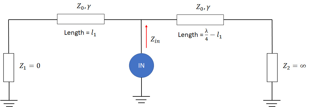
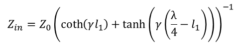
If you set these two legs in parallel and use the standard input impedance equation for each leg, you will find the following result for the antenna’s input impedance:
Once the input impedance is known, it can then be matched to the antenna feedline with an LC impedance matching network.
Component or Copper Fill?
When working in your PCB layout software, should you create your inverted-F antenna as a component or as copper fill regions? There are good reasons to do both, and you will get the same result in either case. Personally, I prefer to use a component to create an inverted-F antenna, but this has to be done to match a specific outer layer thickness and Dk value.
To create an inverted-F antenna as a component, place each of the copper elements in the antenna and poured into the component footprint. Once the antenna is placed into the PCB layout, it will be easier to move and rotate the antenna. Make sure to define the component as a Net Tie to prevent any short circuit errors and to avoid questions from your fabricator. The downside of this is that, if there are any updates needed to the antenna, these need to be made to the footprint, and then the footprint needs to be updated in the PCB layout.

To complete this component, place a single pad as input at the feedline entry on the antenna that matches the pin on the schematic symbol. Then wire the component up in a schematic just like you would other components. Once the components are updated into the PCB, the inverted-F antenna footprint will appear, and it can be placed and routed just like other components.


Leave a Reply
Want to join the discussion?Feel free to contribute!